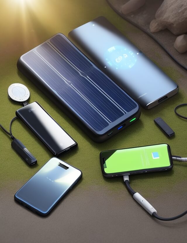
12 Science CBSE11 Science CBSECBSE ProjectsPhysicsPhysics

Physics Project On Semiconductors For Class 11th & 12th CBSE

Acknowledgment

I’d like to extend my heartfelt gratitude to the remarkable individuals and institutions whose unwavering support and contributions made this semiconductor project possible:

My Physics Teacher: My sincerest thanks go to my physics teacher, whose guidance and encouragement have been invaluable throughout this project’s journey. Their expertise and insights have left an indelible mark on the project’s content and direction.

My Classmates: A warm appreciation to my classmates for engaging in thought-provoking discussions and generously sharing their ideas during our brainstorming sessions. Your collective wisdom significantly elevated the quality of this project.

Parents and Family: To my parents and family, I owe an immeasurable debt of gratitude. Their unwavering support, boundless encouragement, and endless patience were the bedrock of my motivation throughout this endeavor.

School Library: The school library, with its treasure trove of resources, played a pivotal role in my research. Special thanks to the librarian for their assistance in sourcing relevant books and materials.

It’s crucial to acknowledge that this project would not have seen the light of day without the cooperative spirit and support of all those mentioned above. Any errors or omissions in this project rest solely on my shoulders.

Warm regards,

[Your Name][Your School Name][Date]

Demystifying Semiconductors: A Gateway to Modern Technology

Enter the world of semiconductors, those unsung heroes of modern electronics and technology. They are the bridge between conductors like metals and insulators such as ceramics or rubber. Semiconductors possess unique properties that stem from their ability to selectively conduct electrical current, a foundational element of the electronic devices we can’t imagine our lives without. This introduction serves as your compass, guiding you into the realm of semiconductors, unraveling their properties, and unveiling their significance in the grand tapestry of physics and technology.

Unraveling the Semiconducting Mystery

Imagine materials that don’t quite fit the bill of conductors or insulators but dance gracefully in the middle, exhibiting what we call intermediate electrical conductivity. These are semiconductors. Unlike conductors that welcome the flow of electrical current or insulators that staunchly resist it, semiconductors have a magical trick up their sleeves – the ability to tweak their conductivity in response to temperature, light, or the presence of impurities. This chameleon-like quality makes them the darlings of the electronics world.

Crystalline Symphony: Semiconductor Structure

Semiconductors often don a crystalline attire, with their atoms meticulously arranged in an elegant, ordered pattern. Silicon (Si) and germanium (Ge) take center stage as the go-to semiconductor maestros in the world of electronics, thanks to their impeccable crystalline performance.

The Energy Ballet: Band Structures

To grasp the essence of semiconductors, you must acquaint yourself with their energy band structure. Picture two bands on the stage: the valence band, where electrons are dutifully bound to atoms, and the conduction band, where electrons break free to conduct electricity. The magic lies in the bandgap – the energy gulf between these bands. A small gap allows electrons to leap from the valence band to the conduction band with ease, transforming the material into a conductor. A wide gap, on the other hand, spells insulation. Semiconductors strike a balance with a moderate bandgap, granting them controlled conductivity.

Tailoring with Elegance: Doping

In the world of semiconductors, we have a bespoke tailoring process known as doping. It’s like adding a pinch of spice to the recipe. Doping involves introducing tiny quantities of impurities into the crystal structure. There are two star players here: the n-type, with surplus electrons, making it electron-rich and a stellar conductor, and the p-type, boasting an excess of “holes,” which are positive charge carriers in disguise.

Semiconductors: The Digital Artisans

Now, imagine a world without transistors, diodes, integrated circuits, or microprocessors. Impossible, right? Semiconductors are the unsung artisans behind these marvels of modern technology. They are the maestros who orchestrate the control and manipulation of electrical currents, paving the way for compact, efficient, and powerful electronic systems.

A Canvas of Possibilities

The applications of semiconductors span across the vast landscape of human innovation. From computing and telecommunications to renewable energy and healthcare, semiconductors are the invisible threads that weave technological wonders. They power solar cells, illuminate LEDs, give life to lasers, and lend their sensitivity to sensors, all shaping the world we inhabit.

In this expedition, we embark on a journey to unravel the enigmatic world of semiconductors, decipher the physics governing their behavior, explore the art of fine-tuning their electrical characteristics, and witness their pivotal role in a myriad of electronic devices and applications. A deeper understanding of semiconductors is the key to unlocking the mysteries of the technological revolution that surrounds us.

Unveiling the Microcosmos: Atomic Structure and the Magic of Semiconductors

Peering into the heart of semiconductors requires a journey through their atomic terrain, where the dance of electrons and nuclei sets the stage for their unique electrical properties. In this chapter, we embark on an atomic odyssey, deciphering the building blocks of semiconductors and how these intricacies give rise to their role as materials with intermediate conductivity.

1. The Atomic Ensemble of Semiconductors:

Picture semiconductors like silicon (Si) or compounds like gallium arsenide (GaAs) as the performers on this atomic stage. The drama unfolds with the following cast:

  • Atomic Nucleus: At the nucleus’s core lies a minuscule but dense assembly of protons (positively charged) and neutrons (neutral). It’s the number of protons that stamps an element’s identity, while the protons and neutrons together dictate its atomic mass.
  • Electron Cloud: Enveloping this nucleus is an ethereal cloud of electrons (negatively charged) engaged in a cosmic ballet. These electrons reside in energy levels and subshells, each with its distinctive energy and spatial fingerprint.

2. The Valiant Valence Electrons:

In our semiconductor saga, the outermost electrons, the valence electrons, emerge as the protagonists. Their count determines how an atom interacts with its atomic comrades, influencing both chemical bonds and electrical conductivity.

3. A Bond of Sharing: Covalent Bonding

In the semiconductor realm, elements like silicon take center stage by forming a crystalline web through covalent bonding. Here, atoms share their valence electrons, a communal act that fashions a sturdy, lattice-like structure in the crystal.

4. The Ballad of Energy Bands and the Bandgap:

To decipher the semiconductor symphony, you must acquaint yourself with its energy bands:

  • Valence Band: This band cradles the valence electrons, where they are tethered to their parent atoms in a loving embrace.
  • Conduction Band: Above the valence band, the conduction band awaits, initially unoccupied. It is a realm where electrons roam freely, contributing to the material’s electrical conductivity.
  • Bandgap (The Grand Canyon of Energy): The bandgap, a chasm of energy between the valence and conduction bands, stands as the pivotal element. It signifies the energy hurdle electrons must leap to escape the valence band’s clutches. Semiconductors sport a moderate bandgap, larger than conductors but narrower than insulators, a sweet spot for controlled conductivity.

5. The Core of Intrinsic Semiconductors:

Enter the pristine world of intrinsic semiconductors, untouched by the hand of doping. Their electrical tale is woven primarily by temperature and the intrinsic bandgap.

6. Crafting Excellence: Extrinsic Semiconductors and the Art of Doping

For a bespoke semiconductor experience, we introduce extrinsic semiconductors through a process known as doping. This is where the maestros of semiconductor manipulation shine:

  • N-type Doping: Elements like phosphorus or arsenic grace the stage, bringing along their surplus electrons, turning the crystal into an electron-rich, n-type masterpiece.
  • P-type Doping: Elements like boron or aluminum make their entrance, introducing a dearth of electrons into the silicon lattice, creating holes and orchestrating a p-type, hole-rich spectacle.

7. Charge Carriers:

In this captivating show, charge carriers take center stage. They are the electrons (in n-type) or holes (in p-type) that respond to an applied electric field, choreographing the material’s electrical conductivity.

With the atomic secrets and the bandgap elucidated, you now possess the key to unlock the door to the semiconductor’s enigmatic world. In the forthcoming acts of your project, you will delve into how doping influences conductivity, explore the wondrous devices born of semiconductors, like diodes and transistors, and witness their transformative role in the grand theater of electronics.

Demystifying Semiconductors: Intrinsic and Extrinsic Variations

In the mesmerizing realm of semiconductors, we encounter two distinct characters: the pure-hearted “Intrinsic” and the artfully crafted “Extrinsic.” Let’s embark on a journey to fathom their unique qualities, unraveling the secrets behind their electrical prowess.

Intrinsic Semiconductors:

Character Portrait:

  • Pure Essence: Intrinsic semiconductors, exemplified by silicon (Si) or germanium (Ge), are the virtuous souls of the semiconductor world, unaltered by the hand of intentional doping or impurities.
  • Crystal Clarity: Their crystalline structures are pristine, with atoms engaging in harmonious covalent bonds, forming an ordered lattice.
  • Valence Virtuosos: The show is run by valence electrons, the virtuosos of intrinsic semiconductors. These electrons in the outermost shell call the shots.
  • Bandgap Ballet: Central to their tale is the energy bandgap (Eg), a portal between the valence and conduction bands. It’s a small gap, larger than conductors but smaller than insulators, allowing electrons to engage in a delicate dance.
  • Chilly Beginnings: At frigid temperatures, intrinsic semiconductors are reluctant to conduct, with only a handful of electrons in the conduction band.
  • Thermal Awakening: As the temperature rises, the electron population in the conduction band swells as thermal excitement takes center stage.
  • Balanced Ensemble: Intrinsic semiconductors maintain harmony; there’s no favoritism between electrons and holes. They coexist in equilibrium.

Extrinsic Semiconductors:

Character Portrait:

  • The Doping Drama: Extrinsic semiconductors are the result of a thrilling “doping” process. Intentional impurities, known as dopants, enter the scene.
  • N-Type Stars: Phosphorus and arsenic, the headliners for n-type doping, bring their extra electrons to the party, making it an electron-rich affair.
  • P-Type Maestros: Boron and aluminum take the stage for p-type doping, creating vacancies or “holes” that twirl gracefully through the crystal, lending it a positive charge.
  • Conductivity Tailored: Extrinsic semiconductors grant us the power to mold their conductivity. N-type and p-type materials, with their contrasting electron abundance or hole abundance, allow for precise control.
  • Charge Carriers in the Spotlight: Electrons (n-type) or holes (p-type) seize the limelight as dominant charge carriers, simplifying the narrative of electrical current flow.
  • Temperature Consistency: Unlike the temperamental intrinsic semiconductors, extrinsic varieties exhibit linear temperature-dependent conductivity, behaving predictably.

In this grand saga of semiconductors, extrinsic semiconductors take center stage, driving the creation of pivotal devices like diodes and transistors. By playing with the electron and hole symphony through strategic doping, we bend these materials to our will, sculpting the foundations of the technological wonders that shape our world.

Semiconductor Enchantments: Unveiling the Magic of Electronic Components

In the mystical realm of electronics, semiconductor devices reign supreme, wielding their unique powers to shape the world of technology. These enchanting components have woven themselves into the very fabric of modern life. Let’s embark on a journey to discover these devices and the wonders they bring:

Diodes:

Character Portrait:

  • Gatekeepers of Current: Diodes, with their two terminals, act as guardians of the electron realm, allowing current to flow in one direction only.

Magical Applications:

  • Rectification Spells: Diodes work their magic by converting the ebb and flow of alternating current (AC) into the steady current of direct current (DC).
  • Signal Clipping Tricks: They are also skilled in the art of signal clipping, limiting the amplitude of AC signals.
  • Voltage Regulation Charms: In the form of Zener diodes, they maintain a constant voltage output, like wizards maintaining the balance of the universe.

Transistors:

Character Portrait:

  • Three-Terminal Wizards: Transistors, the three-terminal sorcerers, possess the power to amplify and switch electronic signals.

Magical Applications:

  • Amplification Spells: They amplify feeble signals, adding strength to their voice in the world of electronics.
  • Switching Incantations: Transistors transform into electronic switches, performing their binary dance in digital logic circuits and computers.

Integrated Circuits (ICs):

Character Portrait:

  • The Masters of Miniaturization: Integrated circuits, or microchips, are grandmasters in the art of cramming thousands to millions of electronic components onto a single chip.

Magical Applications:

  • Shrinking Enchantments: They reduce the size of devices like no other, giving us pocket-sized wonders like smartphones and microcontrollers.
  • Versatile Wizardry: ICs serve in various roles, from the sage microprocessors to the memory mavens, sensors, and communication conjurers.

Light-Emitting Diodes (LEDs):

Character Portrait:

  • Luminous Spellcasters: LEDs are semiconductor devices that emit light as if by pure magic when touched by an electric current.

Magical Applications:

  • Radiant Illumination: They enchant us with their illumination in displays, indicators, lighting fixtures, and optical communication.
  • Eco-Friendly Elegance: LEDs are eco-sorcerers, reducing energy consumption and replacing outdated incandescent bulbs.

Photovoltaic Cells (Solar Cells):

Character Portrait:

  • Sunlight Sorcery: Photovoltaic cells harness the power of sunlight, converting it into electrical energy through the secrets of semiconductors.

Magical Applications:

  • Solar Magic: They create energy from the sun’s rays, fueling the movement towards renewable energy sources and reducing our reliance on fossil fuels.

Thyristors (SCRs and Triacs):

Character Portrait:

  • High Voltage Enchanters: Thyristors, including SCRs and Triacs, are semiconductors skilled in controlling high voltage and current.

Magical Applications:

  • Power Regulation Spells: They take the helm in applications where the control of high voltage and current is a necessity, orchestrating motor control and power regulation.

Field-Effect Transistors (FETs):

Character Portrait:

  • Electric Field Sages: FETs, with their field-effect prowess, elegantly manipulate the flow of current using electric fields.

Magical Applications:

  • Energy-Efficient Elixirs: MOSFETs, in particular, are known for their low power consumption, making them a vital ingredient in the elixir of portable devices like smartphones.
  • Frequency Sorcery: FETs reign supreme in high-frequency domains, like the guardians of radio frequency amplifiers and mystical microwave devices.

These semiconductor enchantments, among others, are the heart and soul of modern electronics. Their spells and charms have ushered in the age of communication, computing, and clean energy. Understanding their mystical workings is the key to unlocking the secrets of this electronic wonderland.

The Inner Workings of Semiconductor Marvels

Delving into the intricate mechanisms of semiconductor devices unveils the essence of their functionality and their pivotal roles in electronic circuits. Below, we embark on a journey to fathom the working principles of some common semiconductor devices:

Diodes:

  • The Diode’s Dance: Diodes, with their p-n junction, perform a ballet of rectification, allowing current to flow in one direction while gracefully blocking it in the reverse.
  • Forward Elegance: Under forward bias (positive voltage on the p-side and negative on the n-side), the diode lowers the energy barrier at the junction, encouraging electron flow from the n-side to the p-side, ushering in a forward current.
  • Reverse Poise: When reverse-biased (positive voltage on the n-side and negative on the p-side), the diode elevates the energy barrier, discouraging electron movement and creating a subtle reverse leakage current.

Transistors (Bipolar Junction Transistors – BJTs):

  • The BJT Symphony: BJTs, composed of emitter, base, and collector layers, act as conductive conductors or switches.
  • Harmonic Amplification: In an NPN transistor, a small base current orchestrates a grand performance, controlling a much larger collector current. This amplification of current defines the essence of a BJT in active mode.
  • Switching Overture: By applying a modest current to the base, the transistor orchestrates a symphony of current flow from the collector to the emitter, functioning as a switch with grace.

Field-Effect Transistors (FETs – MOSFETs):

  • The FET Sonata: FETs dance to the tune of an electric field, modulating the conductive channel between source and drain terminals.
  • MOSFET Movement: In Metal-Oxide-Semiconductor Field-Effect Transistors (MOSFETs), a gate terminal, separated by a thin oxide layer, wields an electric field that guides the flow of charge carriers between source and drain.
  • Modes of Conductivity: MOSFETs, whether N-channel or P-channel, embrace two modes: enhancement (normally off, awakened by gate voltage) and depletion (normally on, lulled into dormancy by gate voltage).

Light-Emitting Diodes (LEDs):

  • The LED Waltz: LEDs, born of semiconductors, cast their radiant glow through electron-hole reunions.
  • Electron Luminescence: When voltage graces the LED, electrons in the conduction band unite with holes in the valence band, creating a luminous spectacle as they release photons. The color of this luminescence is dictated by the semiconductor’s energy bandgap.

Photovoltaic Cells (Solar Cells):

  • The Solar Cell Serenade: Photovoltaic cells serenade the sun’s photons, coaxing them into a dance that converts sunlight into electrical energy.
  • Semiconductor Sorcery: Typically silicon, the chosen semiconductor, captures photons, elevating electrons from the valence band to the conduction band, where electron-hole pairs form.
  • Electric Harvest: These separated electrons and holes are gracefully collected by the cell’s contacts, yielding a harmonious symphony of electric current and voltage.

Understanding these enchanting workings lays the foundation for crafting, analyzing, and mending electronic circuits and systems that embrace semiconductor devices. From the simplicity of diode rectification to the complexity of transistor amplification and the radiance of LED illumination, these devices are the bedrock of modern technology’s grand symphony.

Semiconductors Unveiled: Catalysts of Innovation

Semiconductors, the unsung heroes of our technological era, have woven their influence into a plethora of industries and applications, reshaping our world in profound ways. Let’s illuminate the diverse and impactful applications of these remarkable materials:

Electronics:

  • Integrated Circuits (ICs): Semiconductors power the brains of our devices, enabling the existence of microchips that drive computers, smartphones, and a gamut of digital marvels.
  • Transistors: These versatile components find homes in digital logic circuits, amplifiers, and signal processors within our electronic gadgets.
  • Diodes: Diodes serve as gatekeepers, facilitating rectification, voltage regulation, and signal control in electronic circuits.

Communication:

  • Semiconductor Lasers: The backbone of optical communication, these lasers propel data across fiber optics, and power the laser diodes in our CD/DVD players.
  • Radio Frequency (RF) Devices: Semiconductors empower RF amplifiers and oscillators, critical for wireless communication systems.

Optoelectronics:

  • Light-Emitting Diodes (LEDs): LEDs illuminate our world, gracing displays, indicators, lighting, and displays with energy-efficient radiance.
  • Photodetectors: These sensors, rooted in semiconductors, facilitate light sensing applications in optical communication and imaging systems.

Solar Energy:

  • Photovoltaic Cells (Solar Cells): Semiconductors harness the sun’s energy, offering clean and renewable power through solar panels.

Power Electronics:

  • Power Diodes and Thyristors: These components rectify power, regulate voltage, and orchestrate high-power switching in electrical grids and power electronics.
  • Insulated Gate Bipolar Transistors (IGBTs): IGBTs reign in high-voltage, high-current domains, propelling motor drives and inverters.

Sensing and Detection:

  • Semiconductor Sensors: From temperature to pressure, gas to motion, these sensors find homes in automotive, industrial, and consumer electronics, enhancing our lives through data.

Medical Devices:

  • Semiconductor-based Imaging: Semiconductors empower imaging technology in medical devices such as X-ray machines, MRI scanners, and ultrasound devices.

Aerospace and Defense:

  • Semiconductor Electronics: From avionics to radar and missile guidance systems, semiconductors provide the foundation for cutting-edge technology.
  • Infrared Sensors: Semiconductor-based infrared detectors enable thermal imaging and night vision, enhancing security and surveillance.

Automotive Industry:

  • Engine Control Units (ECUs): Semiconductors take the wheel in engine control, safety systems, infotainment, and navigation, shaping the driving experience.
  • Electric Vehicles (EVs): Semiconductor technology fuels the propulsion and control systems of electric vehicles, steering us toward a sustainable future.

Consumer Electronics:

  • Smartphones and Tablets: Our ubiquitous companions rely on semiconductors for microprocessors, memory chips, touchscreens, and sensors.
  • Flat-Panel Displays: Liquid crystal displays (LCDs) and organic light-emitting diode displays (OLEDs) leverage semiconductors for pixel perfection.

Industrial Automation:

  • PLCs (Programmable Logic Controllers): These orchestrators of industry employ semiconductors for automation and precision control.

Internet of Things (IoT):

  • Wireless Sensors and Communication: In the realm of IoT, semiconductors facilitate wireless data transmission and processing, fostering smart homes, cities, and industries.

Semiconductors, the unsung champions of our modern age, reign supreme in myriad applications. Their adaptability, precision, and mastery over electrical signals have transformed our existence, redefining how we work, communicate, generate energy, and shape the future.

The Precision Craftsmanship of Semiconductor Fabrication

Semiconductor fabrication, often known as semiconductor manufacturing or processing, is an intricate dance of precision and innovation that births integrated circuits (ICs), microchips, and a myriad of semiconductor devices. This meticulously orchestrated process unfolds through the following pivotal stages:

Crystal Growth:

  • Monocrystalline Silicon: It all begins with the birth of monocrystalline silicon wafers. A seed crystal takes a dip in molten silicon and is delicately drawn, giving birth to a single crystal ingot, which is then sliced into thin wafers.

Wafer Preparation:

  • Wafer Polishing: Silicon wafers are meticulously polished to achieve a flawlessly smooth surface.
  • Cleaning: The wafers undergo a rigorous cleansing process, purging them of any contaminants.

Silicon Doping:

  • Ion Implantation: To orchestrate the electrical properties of silicon, dopant ions are implanted into the wafer’s surface. This introduces a surplus of electrons (n-type doping) or electron deficiencies (p-type doping), crafting distinct electrical traits in different regions.

Oxidation:

  • Thermal Oxidation: A layer of silicon dioxide (SiO2) is meticulously nurtured on the wafer’s surface through exposure to high-temperature oxygen or water vapor. This silicon dioxide layer stands as an insulating dielectric in transistors and other electronic components.

Photolithography:

  • Photoresist Coating: A photosensitive photoresist material blankets the silicon wafer’s surface.
  • Mask Alignment: A photomask, bedecked with the desired circuitry pattern, aligns gracefully above the wafer.
  • Exposure: Ultraviolet light pours through the photomask, mirroring the pattern onto the photoresist.
  • Developing: Unexposed regions of the photoresist are tenderly coaxed away, leaving the pattern imprinted on the wafer.

Etching:

  • Chemical Etching: Exposed segments of the silicon wafer are delicately chemically etched to shape or remove silicon material, adhering to the photoresist’s design.

Ion Implantation (Additional):

  • Threshold Adjustment: In certain cases, supplementary ion implantation steps come into play to fine-tune doping levels in precise regions of the chip.

Thin-Film Deposition:

  • Chemical Vapor Deposition (CVD): Thin layers of materials, be it metals for interconnections or dielectrics for insulation, are gently laid upon the wafer’s surface through meticulously controlled chemical reactions.

Photolithography (Additional):

  • Multiple Patterning: In advanced semiconductor realms, multiple photolithography steps are summoned, conjuring intricate patterns on a smaller scale.

Chemical Mechanical Polishing (CMP):

  • Planarization: CMP sweeps in, bestowing a flat and velvety finish to the wafer post each layer addition, ensuring precision in layer alignment.

Interconnect Formation:

  • Metal Layers: Multiple metal layers are gently deposited and patterned to craft intricate interconnections between distinct components on the chip.

Annealing:

  • Heat Treatment: Annealing sweeps in, activating dopants and mending any imperfections within the silicon lattice.

Testing and Inspection:

  • Wafer Testing: Each chip upon the wafer undergoes meticulous tests, ensuring both functionality and quality.
  • Defect Inspection: Refined inspection tools come into play, sifting through the wafer to spot and pinpoint any aberrations.

Wafer Dicing:

  • Individual Chip Separation: The wafer is carefully segmented into individual chips, each cradling a solitary integrated circuit.

Packaging:

  • Encapsulation: These chips are delicately cocooned within protective encasements, shielding them from the elements and the rigors of handling.

Final Testing:

  • Functional Testing: Each ensconced chip undergoes a final rite, where its functionality is scrutinized to meet stringent performance benchmarks.

Distribution:

  • Packaged Devices: The culmination of this grand endeavor is the delivery of fully functional semiconductor devices to manufacturers, who in turn weave them into an array of electronic creations.

Semiconductor fabrication, a symphony of precision and innovation, is a transformative crucible. With each advancement in this craft, our devices become faster, smaller, and more energy-efficient. It is the heartbeat of our modern age, a crucial lynchpin in industries from electronics to healthcare and aerospace, ushering in a world of technological marvels.

Future Trends in Semiconductor Technology

The realm of semiconductor technology remains in a perpetual state of transformation, driven by our ceaseless hunger for faster, more energy-efficient, and smaller electronic marvels. Here, we glimpse into the promising future trends:

1. Miniaturization Beyond Moore’s Law:

  • Post-FinFET Era: The inexorable march towards atomic limits compels us to explore novel transistor designs and materials. Gate-all-around (GAA) and nanosheet transistors are emerging champions, aiming to prolong Moore’s Law and continue our miniaturization odyssey.
  • Quantum Computing: In the quantum arena, a seismic shift beckons. Quantum computers, harnessing the enigmatic principles of quantum mechanics, harness quantum bits (qubits) to tackle once-impenetrable challenges, promising a transformative leap in computing capability.

2. Advanced Materials:

  • 2D Wonders: The enchanting world of 2D materials, including graphene and transition metal dichalcogenides (TMDs), tantalizes us with their unique electronic virtues, potentially becoming integral in future semiconductor wonders.
  • Compound Semiconductors: Gallium nitride (GaN) and silicon carbide (SiC) rise as triumphant contenders, bolstering power electronics, high-frequency applications, and even infiltrating select realms of microelectronics, flaunting their superior prowess.

3. Neuromorphic and AI Hardware:

  • Neuromorphic Wonders: Neuromorphic computing scripts a grand narrative, mimicking the neural intricacies of our minds. Specialized AI chips promise to transform the landscape of AI processing, tailored for distinct applications.

4. 3D Integration:

  • Embracing the Third Dimension: We navigate vertical horizons as three-dimensional integration, stacking semiconductor layers skyward, shortening interconnects, and orchestrating superior performance and energy frugality.

5. Advanced Packaging:

  • Packaging Evolution: Advanced packaging techniques, from chiplets to system-in-package (SiP) to heterogeneous integration, dance onto center stage, resolving the conundrums of heat, power, and bandwidth.

6. Power Electronics on the Horizon:

  • Wide-Bandgap Brilliance: Wide-bandgap materials like SiC and GaN enchant power electronics, where efficiency reigns supreme, heat dissipates into oblivion, and higher frequencies beckon.

7. Quantum Dots:

  • Quantum Dot Radiance: Quantum dots elegantly grace displays, elevating color precision, brilliance, and energy thriftiness. The future promises further enhancements in display technology.

8. Memory Technologies:

  • Non-Volatile Magic: Emerging non-volatile memory forms, such as Resistive RAM (RRAM) and Phase-Change Memory (PCM), bear the torch for denser, lower-power memory solutions, transcending the limits of traditional Flash memory.

9. Edge Computing:

  • Edge AI Renaissance: The crescendo of AI at the edge reverberates. Specialized AI accelerators and energy-savvy processors step forth, empowering a world of autonomous vehicles and IoT devices.

10. Sustainable Horizons:

  • Green Commitment: The semiconductor industry forges a path towards sustainability, embracing eco-friendly manufacturing processes and material recycling.

11. Security and Privacy:

  • Sentinels of Hardware: As the digital realm grapples with ever-evolving cybersecurity threats, hardware security features take center stage, ensuring data sanctity and privacy.

12. Quantum-Proof Cryptography:

  • Guarding Against Quantum Dawn: Anticipating the day quantum computers challenge existing encryption, the realm of post-quantum cryptography emerges, crafting algorithms and hardware solutions to shield our digital fortresses.

These future trajectories of semiconductor technology beckon with innovation and transformation. Material breakthroughs, architectural innovations, and manufacturing wizardry are poised to redefine our electronic, computing, and communication landscapes, unlocking a universe of possibilities across industries.

Challenges and Limitations of Semiconductor Devices

Semiconductor devices have ushered us into an era of technological marvels, yet they confront a tapestry of challenges and limits. Here are the key hurdles and confines intertwined with these ingenious creations:

1. Miniaturization Limits:

  • Physical Boundaries: As we voyage toward atomic scales, quantum quirkiness emerges, testing the boundaries of predictability and reliability.
  • Thermal Trials: Miniaturization begets potent power densities, birthing an inferno of heat. Managing this thermal tempest becomes paramount to uphold device longevity and prowess.

2. Power Consumption:

  • Leakage Labyrinth: As transistors dwindle, soars the specter of leakage current, siphoning power in idle or dormant states.
  • Energy-Efficiency Quest: The quest to pare power appetites while preserving performance grips the semiconductor realm, especially in battery-powered realms and data sanctuaries.

3. Interconnect Predicaments:

  • Resistance and Capacitance Quandaries: As chips compress and cluster, resistance and capacitance in the interconnections become foes, heralding signal delays and diminished vigor.
  • Signal Vigilance: Swift communiques between components beckon advanced interconnect arts, safeguarding signal fidelity and mitigating data transmission woes.

4. Reliability:

  • Electromigration Enigma: Over time, the atomic ballet within conductive paths may birth electromigration, orchestrating device obituaries.
  • Wear and Tear Drama: Mechanical duress and thermal symphonies can stage structural and material exhaustion, truncating a device’s voyage.

5. Manufacturing Mayhem:

  • Complex Choreography: Semiconductor crafting dances to the rhythm of precision and complexity, birthing a grand tapestry of intricacies and costs.
  • Yield Yarns: The yield tapestry in fabrication weaves tales of defects and hitches, yielding resources to the relentless void.

6. Materials Meanderings:

  • Material Mysteries: The quest for materials that can sate the appetites of advanced devices is an uncharted expedition. The hunt for new materials with coveted traits persists.

7. Security Stakes:

  • Hardware Havens: Semiconductor devices may harbor vulnerabilities to hardware-level onslaughts, such as side-channel intrigues and hardware Trojans.
  • Quantum Query: Quantum computing’s ascendance ushers the specter of encryption’s frailty, posing security enigmas.

8. Environmental Echo:

  • Resource Ripples: The path of semiconductor creation gobbles resources, leaving footprints of water and energy consumption.
  • E-Waste Epoch: Obsolete electronic relics kindle the fires of electronic waste (e-waste) dilemmas.

9. Economic and Supply Chain Sagas:

  • Global Web: Semiconductor manufacturing is woven into a global web, susceptible to perturbations, as recent chip scarcities underscored.
  • Financial Frontiers: The staggering price tags of fabrication facilities (fabs) and research and development can throttle access to cutting-edge realms.

10. Technology Tangling:

  • Heterogeneous Harmonies: Intertwining diverse technologies into a singular chip – think silicon photonics, MEMS, and RF – courts complications, from compatibility conundrums to manufacturing mazes.
  • Scaling Struggles: Maintaining uniform scaling across chip domains with diverse technologies can prove a herculean task.

Conclusion

In conclusion, semiconductor devices have wielded a transformative influence upon the realm of electronics and technology, bestowing upon us the potent and versatile companions that have seamlessly interwoven themselves into our daily existence. From the computational might of microprocessors gracing our computing devices to the radiant illumination emanating from LEDs adorning our screens, semiconductors have claimed a pivotal role in the tapestry of modern technology.

Our voyage through the labyrinth of semiconductor exploration has unraveled their intricate atomic choreography, demystified the principles governing their conduct, and acquainted us with the diverse species of semiconductor progeny driving our tech-driven civilization. Furthermore, we’ve marveled at their far-reaching applications, spanning the domains of communication, energy generation, healthcare, and automotive engineering.

Gazing toward the horizon, semiconductor technology continues its ceaseless evolution, relentlessly pushing the frontiers of miniaturization, energy thriftiness, and computational prowess. Quantum computing, the allure of advanced materials, and innovative packaging techniques stand poised to reshape the semiconductor landscape in the imminent future.

Yet, let us not be beguiled by the allure of boundless potential; instead, we must remain cognizant of the challenges and constraints encircling the semiconductor realm. These include the shackles of miniaturization, the specter of insatiable power cravings, and the somber echoes of environmental consequences. Vanquishing these adversaries demands ongoing research, steadfast investments, and harmonious collaboration among the guardians of the semiconductor realm.

In essence, the universe of semiconductors is a dynamic symphony, a perpetual overture heralding innovation and molding our technological destiny. As we deftly navigate the labyrinthine challenges and harness the latent powers of nascent technologies, semiconductors will persist as the bedrock upon which our progressively interconnected and digital world is founded.

Certificate of Completion

[Student’s Name][Class/Grade Level]

This is to certify that I, [Student’s Name], a [Class/Grade Level] student, have successfully completed the project on “Semiconductors For Class 11th & 12th CBSE.” The project explores the fundamental principles and key aspects of the chosen topic, providing a comprehensive understanding of its significance and implications.

In this project, I delved into in-depth research and analysis, investigating various facets and relevant theories related to the chosen topic. I demonstrated dedication, diligence, and a high level of sincerity throughout the project’s completion.

Key Achievements:

Thoroughly researched and analyzed Phyics Project On Semiconductors For Class 11th & 12th CBSE.
Examined the historical background and evolution of the subject matter.
Explored the contributions of notable figures in the field.
Investigated the key theories and principles associated with the topic.
Discussed practical applications and real-world implications.
Considered critical viewpoints and alternative theories, fostering a well-rounded understanding.
This project has significantly enhanced my knowledge and critical thinking skills in the chosen field of study. It reflects my commitment to academic excellence and the pursuit of knowledge.

Date: [Date of Completion]Signature: [Your Signature] [School/Institution Name][Teacher’s/Examiner’s Name and Signature]

Click to rate this post!
[Total: 0 Average: 0]

Download Physics Project On Semiconductors For Class 11th & 12th CBSE PDF


Leave a Reply

Your email address will not be published. Required fields are marked *

Back to top button